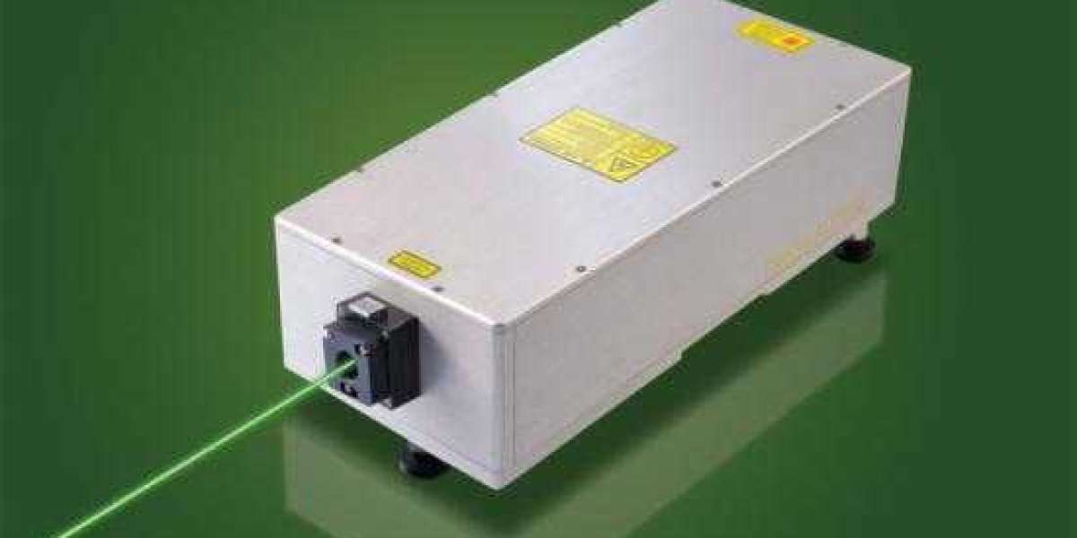
The High power 532nm laser is used to drill through holes. The performance of this process depends on the properties of the material. To maximize productivity, perforation is performed in two steps: ablation of the copper layer at high energy densities of laser radiation (about 4 J/cm2 ) , then perforation of the non-conductive substrate with radiation at a lower energy density (100 mJ/cm2). This sequence provides the smallest heat-affected zone when exposed to the substrate material, thereby making it possible to obtain holes of the best quality: 30 micrometers in diameter, the perforation rate can reach 250 holes per second. In addition, during this exposure, the adhesive properties of the copper surface are improved as a result of laser structure, which has a good effect on the subsequent coating. CO2 lasers, with their usual beam diameter of 70 μm and a large heat-affected zone, do not allow such results to be achieved.
Flexible printed circuit boards are one or more dielectric layers with an electronic circuit formed on it. The production of printed circuit boards from flexible materials expands the possibilities of their application due to design flexibility, lower weight, higher packing density, resistance to dynamic and thermal loads and makes them the best way to interconnect in electronics. Mechanical methods of cutting this form too wide a cut and create high mechanical stresses that are unacceptable for circuits with a complex topology. Cutting with a CO2 laser has a large heat-affected zone and results in carbonization. In addition, CO2 radiation-lasers are completely reflected by metals, which makes it impossible to cut flexible printed circuit boards with metal circuits. UV laser cutting allows high quality cutting of flexible printed circuit boards. Figure 6 shows examples of PCB cutting with CO 2 laser and UV laser. When cutting with a CO2 laser, there are traces of carbonization of the material; when cutting with High power 532nm laser, there is a clean, even cut edge.


